20+ intel 4004 block diagram
Testing and Deployment of Intelligent Object Framework Intelligent Object FrameworkIOFis a platform. Such a feat of integration was made possible by the use of the then-new silicon gate technology which.

Truthtable Of The Majority Function Download Scientific Diagram
4001 - 256-bit mask ROM and 4-bit IO device 4002 - 320-bit RAM and 4-bit IO device 4003 -.

. Also all registers of sytem RAM and ROM are emulated. Innovations in Intel Stratix 10 FPGAs and SoCs 13. This image below was made from new mask data verified by Lajos Kintli using Fred Huettig schematics and Intel scans.
The full code of this software is completely written in JavaScript so it should be able to execute on. The e4004 emulator is a very complex emulator of the INTEL 4004 system. FPGA and SoC Features Summary 14.
The Intel 4004 was a part of MCS-4 chipset which included the following chips. This became the MCS-4 Micro Computer System project. Memory Program memory size is 4 KB.
The demonstration board showcases the features of the Intel Agilex I-Series device in the F2957 FBGA package. Intel Corporation The Intel 4004 chip made its debut in November 1971. The following are photographs of Federicos original schematics for the 4004 in 3 sheets with hand notations in pencil by Federico.
The Memory Block containing the index registers. Unconditional jump and jump to. All register and flags of CPU block are emulated.
SwItches displays A-O converters. Intel Stratix 10 GXSX Family Variants 12. All conditional instructions work within currently selected ROM 256 bytes.
SPI Controller Signal Description 204. SPI Block Diagram and System Integration 203. 4004 is a complete 4-blt parallel central processing unit CPU easIly Interfaces with keyboardS.
Intel 4004 architectural block diagram 7. Hoff and Stanley Mazor also of Intel and with help from Busicoms Masatoshi Shima came up with the architecture for. Missing vias and non-electrical details Click on the image.
Intel Stratix 10 Block Diagram 15. A schematic diagram offers details of the Intel 4004 microprocessor. 2021 FIXED AUDIO REMASTER.
Download scientific diagram Intel 4004 Microprocessor 1971 6 from publication. The as4004 assembler is a very simple 2 pass assembler of the Intel 4004 microprocessor. After completing the verification work for the 4004 microprocessor I yearned to simulate a complete microcomputer set CPU ROMs and RAMs at the transistor level.
Printers and other peripheral equipment The. The 4004 was historys first monolithic CPU fully integrated in one small chip. These devices feature R-tile transceivers with PCIe.

Intel 4004 Google Search Circuit Board Design Intel 4004 Acceleration
Microprocessor Drawing
1
Diagram

The Architecture Of Pentium Microprocessor Computer Architecture Addressing Mode Program Counter

Block Diagram Of Alu Download Scientific Diagram
![]()
Number Of Transistors On Intel S Mainstream Microprocessor Chip 12 Download Scientific Diagram

2 Intel A 4004 In 10 Um Cmos Process 1971 B Skylake In 14 Nm Download Scientific Diagram

Pdf A Review Of Architectures Intel Single Core Intel Dual Core And Amd Dual Core Processors And The Benefits
If Intel Built An Exact Copy Of The Original Z80 Micro Processor Using Today S State Of The Art Manufacturing Technology How Many Times Faster Would It Be Quora

Intel 4004 Things Have Come On A Fair Bit In The Last Fourty Years Intel 4004 Intel Engineering
Cpu Architecture Computer Architecture Electrical Wiring Colours Pic Microcontroller

Airmont Microarchitectures Intel Wikichip Intel Computer History Architecture
1
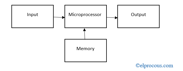
Microprocessor Components Generations And Its Types
What Is The Internal Diagram Of A Cpu Quora

An Intel Board At Moma An Artist Curates Chip Designs Museumzero Circuit Board Design Computer History Old Technology